



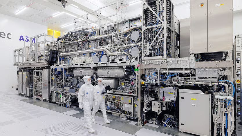
ASML is one of those companies that sounds boring until you understand what it controls.
The company makes lithography machines. These machines print circuit patterns onto silicon wafers. Without lithography, there are no advanced chips. Without advanced chips, there is no serious AI infrastructure, no high-end GPUs, no advanced smartphones, no leading-edge data centers, and no continued push toward smaller, faster, more efficient semiconductors.
That is the simple thesis.
ASML sits in one of the most important parts of the semiconductor manufacturing chain. Its EUV machines are used to produce the most advanced chips in the world, including the chips needed for AI, high-performance computing, advanced memory, and next-generation logic nodes.
The BE Invested Labs ASML report gives the company an Outperform rating, with a probability-weighted fair value estimate of $2,150 per share. At the report price of $1,899.48, that implies around 13.2% upside over a 12 to 24 month horizon. The bull case reaches $2,550. The bear case falls to $1,450.
That range matters.
ASML is a very high-quality company. It is also expensive. The investment debate is not whether ASML is important. The debate is whether today’s valuation still leaves enough room for future returns.
If you want business breakdowns like this in your inbox, subscribe to BE Invested Labs. We break down companies through history, numbers, valuation, risk, and long-term business quality.
Prefer to listen? We generated an AI audio briefing from the full BE Invested Labs ASML research report.
From a leaky shed to the center of the chip industry
ASML started in 1984 as a joint venture between Philips and ASM International. It began life in a leaky shed near Philips’ buildings in Eindhoven, the Netherlands.
That detail matters because ASML was not born as an obvious winner. It was a small Dutch lithography company entering a market with bigger competitors, limited customers, and expensive research needs. ASML’s own history says the company had few customers in the late 1980s and could not stand on its own feet. ASMI withdrew, Philips was cutting costs, and the young company’s future was uncertain.
So before ASML became a European technology giant, it nearly failed.
The first real escape came in the 1990s with the PAS 5500 platform. That system helped ASML win important customers, improve productivity, and move toward profitability. In 1995, ASML became a public company listed in Amsterdam and New York. Philips sold half its stake at the IPO and later sold the rest.
The early 2000s then gave ASML another push. In 2001, the company introduced TWINSCAN, a dual-stage lithography system that could expose one wafer while measuring and aligning another. That improved productivity for customers. In 2003, ASML introduced its first immersion lithography machine. By 2007, it had shipped an immersion system with a numerical aperture of 1.35, the highest in the industry at the time.
This period matters for investors because ASML did not win by accident. The company kept solving specific customer problems: resolution, productivity, throughput, cost per chip, and manufacturing accuracy.
Those wins made ASML stronger before EUV became commercially real.
The EUV bet
EUV stands for extreme ultraviolet. ASML’s EUV systems use light with a wavelength of 13.5 nanometers, which is almost in the x-ray range. That shorter wavelength allows chipmakers to print extremely small and complex layers on advanced chips.
This technology took more than 2 decades to develop. ASML says it invested more than €6 billion in EUV R&D over 17 years. The company also acquired Cymer in 2013 to strengthen its EUV light source capability.
The technical problem was brutal. EUV light is absorbed by air, so the system must operate in a vacuum. The light source fires laser pulses at droplets of tin up to 50,000 times per second. The wafer stage positions wafers within a quarter of a nanometer and checks or adjusts 20,000 times per second.
That is why EUV became a graveyard for competitors.
Many companies explored EUV. ASML kept going. In 2006, it shipped the first EUV demo tools. In 2010, it shipped the first pre-production EUV system. In 2013, it shipped the first production EUV system. In 2016, customers began ordering the NXE:3400 in higher volumes. At the start of 2020, ASML celebrated the 100th EUV system shipment.
